Nurduino: Difference between revisions
m (→Kit components) |
|||
| Line 17: | Line 17: | ||
{| class=wikitable | {| class=wikitable | ||
|- | |- | ||
! amount !! Name !! Location !! Picture | |||
|- | |- | ||
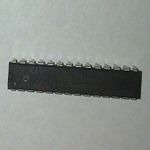
| 1x || | | 1x || Atmega328PU IC || IC3 || [[File:atmega328.jpg|x150px]] | ||
|- | |- | ||
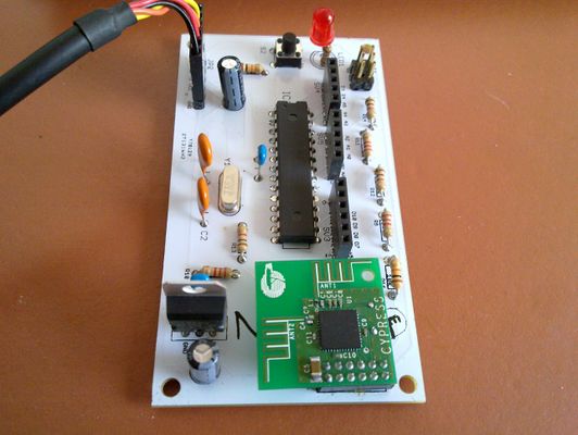
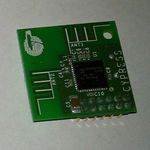
| 1x || | | 1x || CYWM6935 breakout board || in JP1, orientation inside board (see picture above) || [[File:cywm6935.jpg|x150px]] | ||
|- | |- | ||
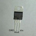
| 1x || | | 1x || LD1117V33 Voltage regulater from 5 (and more) to 3.3V || LD1117V || [[File:LD1117v33.jpg|x150px]] | ||
|- | |- | ||
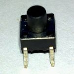
| | | 1x || push button (always off) || S2 || [[File:pushbutton.jpg|x150px]] | ||
|- | |- | ||
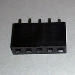
| | | 2x || 5 pin female header || SV4 || [[File:5pin_header.jpg|x150px]] | ||
|- | |- | ||
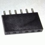
| 1x || | | 1x || 6 pin female header || SV3 || [[File:6pin_header.jpg|x150px]] | ||
|- | |- | ||
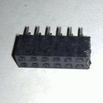
| 1x || | | 1x || 12 pin female header || JP1 || [[File:12pin_header.jpg|x150px]] | ||
|- | |- | ||
| | | 1x || A six pin header (or actually, two 3pin jumpers) || J1 || | ||
|- | |- | ||
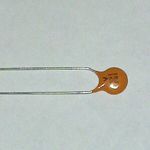
| 2x || | | 2x || 18pF ceramic disc capacitor || C1&C2 || [[File:18pF.jpg|x150px]] | ||
|- | |- | ||
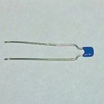
| 2x || | | 2x || 100nF ceramic capacitor || C3&C5 || [[File:100nF.jpg|x150px]] | ||
|- | |- | ||
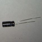
| 2x || | | 2x || 10uF electrolytic capacitor (elco) || The elco places (circles). The oriëntation is important. The short leg of the elco is the minus, and the elco on the pcb has a minus sign at one hole || [[File:10uF.jpg|x150px]] | ||
|- | |- | ||
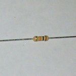
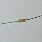
| | | 2x || 10KOhm resistor || R15&R16 || [[File:10k.jpg|x150px]] | ||
|- | |- | ||
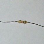
| | | 1x || 1KOhm resistor || R12&R13&R14 || [[File:1k.jpg|x150px]] | ||
|- | |- | ||
| | | 3x || 2.2KOhm resistor || R9&R10&R11 || [[File:2k2.jpg|x150px]] | ||
|- | |- | ||
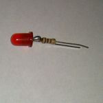
| 1x || 16MHz crystal oscillator || | | 1x || 5mm red LED with integrated 1KOhm resistor || LED1. The oriëntation is important. The long leg on the LED is the + leg. ATTENTION!!! On the PCB the wrong hole is marked with a +. The other hole should contain the + leg of the LED. || [[File:led.jpg|x150px]] | ||
|- | |||
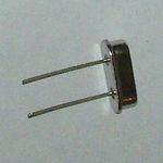
| 1x || 16MHz crystal oscillator || Y1 || [[File:crystal.jpg|x150px]] | |||
|- | |- | ||
|} | |} | ||
Revision as of 01:39, 27 March 2013
| NURDspace Project | |
|---|---|
| Participants | Smokeyd |
| Skills | |
| Status | |
| Niche | |
| Purpose | |
| Tool | |
| Location | |
| Cost | |
| Tool category | |
{{{Name}}}Property "Tool Name" (as page type) with input value "{{{Name}}}" contains invalid characters or is incomplete and therefore can cause unexpected results during a query or annotation process. Property "Tool Image" (as page type) with input value "File:{{{Picture}}}" contains invalid characters or is incomplete and therefore can cause unexpected results during a query or annotation process. {{{Picture}}} {{#if:{{{Tool}}} | [[Tool Owner::{{{ProjectParticipants}}} | }} {{#if:{{{Tool}}} | [[Tool Cost::{{{Cost}}} | }}
Nurduino is our very own arduino clone. It is the evolution of the Arduino Radio Spectrum Analyzer prototype on a breadboard project. In that project I built a prototype of the Nurduino, and tried to share the how's and why's. In this page I will make a shorted description of how to build the Nurduino kit, and use it as a 2.4GHz Radio Analyzer.
What do I need
- A soldering iron (including sponge and stand). Use one that is accurate with a good tip. Although the pcb is setup with a lot of space there are a few spots where accuracy is required. Under €50 there are good options available.
- Solder. I use 0.7mm (more accurate then 1mm) with a resin core, containing lead (was your hands and try not to breathe the fumes).
- FTDI cable or FTDI friend (and micro usb cable) to connect the board to the usb port.
Kit components
Software
- To program the atmega chip, you need this sketch.
- The full schematic and pcb design of the Nurduino can be found in this zipfile.
Putting it together
If this is your first time soldering: don't worry, it is actually not hard. I learnt it from Mitch Altman, who is a great teacher and the co-author of Soldering is easy.

